Laser Full Cut Dicing
Solutions

Compound semiconductors, such as GaAs (Gallium Arsenide), are used in high frequency devices. When blade
dicing compound semiconductors with an existing diamond blade, the feed speed is slow and high
productivity is difficult to obtain.
With the trend towards high integration, based on such technology as SiP (System in Package),
high-strength thin-die manufacturing technology has become necessary. However, with blade dicing, as the
thickness of the wafer becomes thinner, dicing difficulty increases.
To solve this kind of issue, DISCO has optimized the laser head and optical system of the DFL7161 laser saw to establish a laser
full cut application.
Application
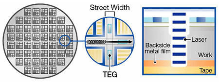
Laser Full Cut Dicing Process
The process involves feeding the laser over the front side (pattern side) of a thinned wafer (less than 200 µm) once, or irradiating the wafer multiple times until a cut is made to the tape. Laser full cut dicing can improve throughput because the feed speed can be increased.
Process example
Thin wafer dicing of the GaAs compound semiconductor
During dicing, breakage and cracking can easily occur in the GaAs wafer because the material is very brittle. Therefore, it has been difficult to increase the feed speed using existing blade dicing. With laser full cut dicing, it is possible to process at feed speeds ten times faster than blade dicing, and thus increase throughput. (This is just an example. The actual speed depends on the wafer to be processed.)
By employing laser full cut dicing, it is possible to realize a reduction in the street width because the kerf width after processing is narrower and the kerf loss compared to blade dicing is less. Compound semiconductors wafers, which tend to have more processing lines to singulate into small die, can increase the number of dies that can be produced from one wafer, by realizing a reduction in the street width.
* When processing GaAs, additional equipment to remove the vaporized As gas is necessary.
Thinned silicon wafer full cut dicing
As wafers become thinner, the chipping and cracking during dicing have a greater influence on the die strength. Therefore, dicing difficulty is increasing because processes that better control chipping are being demanded. Also, the number of devices that use Die Attach Film (DAF) as the bonding material to stack thinned dies is increasing. As a result, high-quality dicing of a wafer, which is attached with DAF on its backside, while controlling the occurrence of burring has become a problem.
In response to this problem, DISCO has established an application that performs full cut dicing with a laser as one of its thin wafer dicing solutions for Silicon. Laser full cut dicing is expected to improve UPH due to the faster processing speed of the laser. Furthermore, for DAF attached Silicon wafers, the Silicon and DAF can either be laser diced together or separately.
-
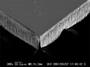
Silicon wafer
Front side die photograph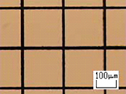
-
DAF attached Silicon wafer
Die side photograph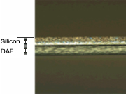
Other laser full cut processing example
Backside metal film attached Silicon wafers, GaP (Gallium Phosphorus) wafers, InP (Indium Phosphorous) wafers, GaN (Gallium Nitride) wafers and Ge (Germanium) wafers.
Process handling equipment
The fully automatic laser saw DFL7161, which supports 300-mm diameter wafers and has an establish reputation for Low-k grooving, has been equipped with an optimized laser head and optical system for the laser full cut dicing specification.

Contact
Please feel free to contact us with any questions or inquiries.
-

Applications Support
A free-of-charge test cut is performed at an application lab to confirm whether achieving the customer's needs is possible.
Details -

Dicing and Grinding Service
It is effective in sample and prototype manufacturing during development or low-volume production. Designated engineers will provide support based on the desired leadtime and at reasonable cost.
Details